Unbeknownst to me, I have gradually approached a significant phase in life, about to step out of the age of wisdom. Simultaneously, I made a significant decision to leave my current company where I had worked for 13 years and venture into a completely new job role. Standing at this juncture, I’ve come to realize that my experiences and journey are worth documenting properly. This record serves multiple purposes, whether it’s preserving cherished memories for myself or offering valuable insights for those who come after me. There’s a certain significance to it all.
Major Choices
Speaking of my career journey, I can’t help but reflect on how I entered the “electronics” industry. Truth be told, there wasn’t much hesitation. After completing my college entrance exam, when it came time to choose a major, I decisively opted for electronics. Back then, the software field didn’t seem as popular, and Yahoo was one of the prominent platforms. Many of the now-familiar applications and websites hadn’t even emerged yet. During that decision-making phase, I did contemplate between electronics, architecture, or civil engineering. I had relatives in the construction industry, and during that era, the demand for architecture and civil engineering was booming. However, I wasn’t keen on following the traditional path. I aspired to explore opportunities in larger cities like Shanghai. Driven by this inner push, I ultimately chose electronics as my major. Thus, my major choice at the time wasn’t heavily influenced by interests or talents, but rather focused on selecting the field that aligned best with my future expectations.
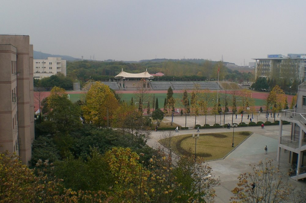
The first three years of my college years in Nanjing were relatively relaxed. That era represented a liberation following the mandatory nine years of education, marked by the introduction of cell phones, the ability to engage in romantic relationships, increased pocket money, and the newfound independence away from parents. My academic performance was average, and I wasn’t a top-performing student. As I approached the end of my third and fourth years, facing graduation, options included pursuing further studies abroad, preparing for postgraduate entrance exams, and for many, entering the workforce. I chose the path of postgraduate studies, as many roles in the industry at that time required a postgraduate degree.
Postgraduate studies narrowed my focus, and I selected the field of ASIC and semiconductors, delving into chip design. When I returned to visit in 2023, I heard that a “Semiconductor School” was being established, highlighting the growing investment in chip education at the institutional level. In the past couple of years, I learned that many institutions that previously didn’t have electronics departments established semiconductor-related programs and schools, taking advantage of the support for the semiconductor industry. While this investment in top-tier institutions offers clear educational direction and resource allocation, a potential drawback is the early separation of electronics and semiconductors. For instance, when I was studying, there were separate departments for radio and electronics. While this categorization may be necessary for knowledge classification, many foundational aspects and curriculum structures among EE-related departments are quite similar.
First Job
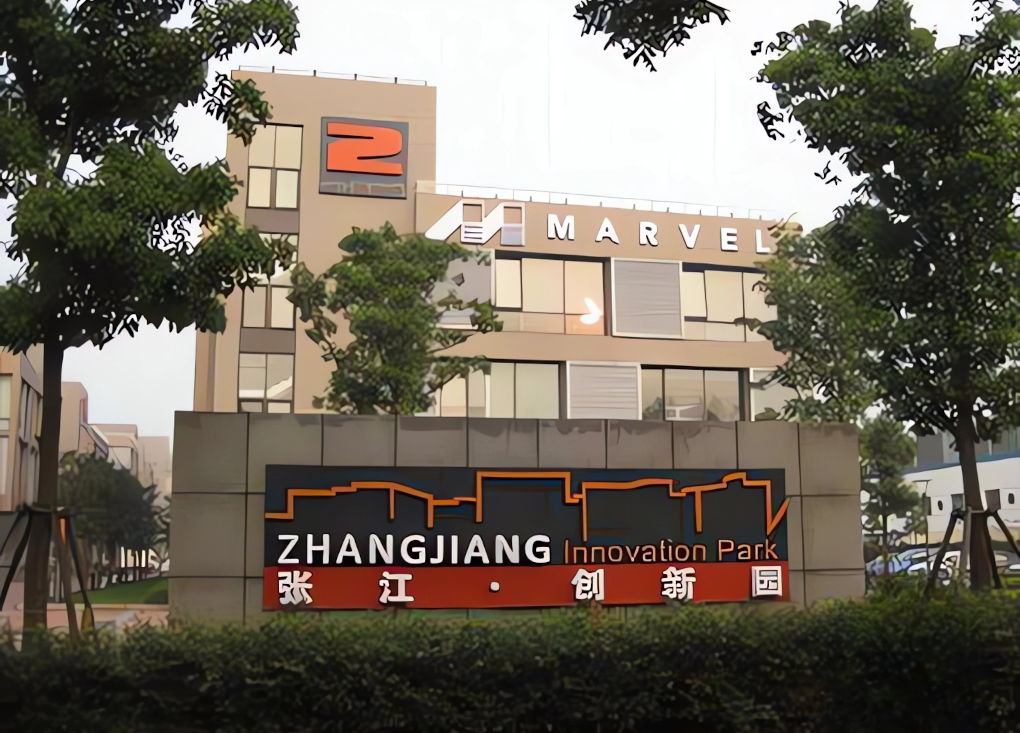
After completing my postgraduate studies, I began my first job, engaging in chip backend design. I was fortunate to be in the right place at the right time. Foreign companies were establishing their presence in China, and resources and technology were flowing into the country, largely attracted by the market size and cost-efficiency. I witnessed China’s transformation from being considered a “low-cost area” by HR to gradually becoming a “high-cost area.” Looking back, the era’s development provided me with opportunities for a starting point and growth. Although I missed out on the semiconductor boom in China, I embarked on a different path in sync with the currents of time. After working in Shanghai for six years, an opportunity arose to transfer to a foreign enterprise in the United States. Without much hesitation, I embarked on a path I had never previously considered: working and living in Silicon Valley.
In my role at the Shanghai branch, I primarily engaged in chip backend design, also known as Chip Physical Implementation Design. The company was actively expanding into China’s baseband chip market and focusing on TD-SCDMA chips, making the workload demanding but the accumulation of experience rapid. Completing various tasks efficiently and reliably was crucial. Due to my interest in automation, I often performed CAD work related to specific projects. This background eventually supported my internal transfer.
Venturing to Silicon Valley
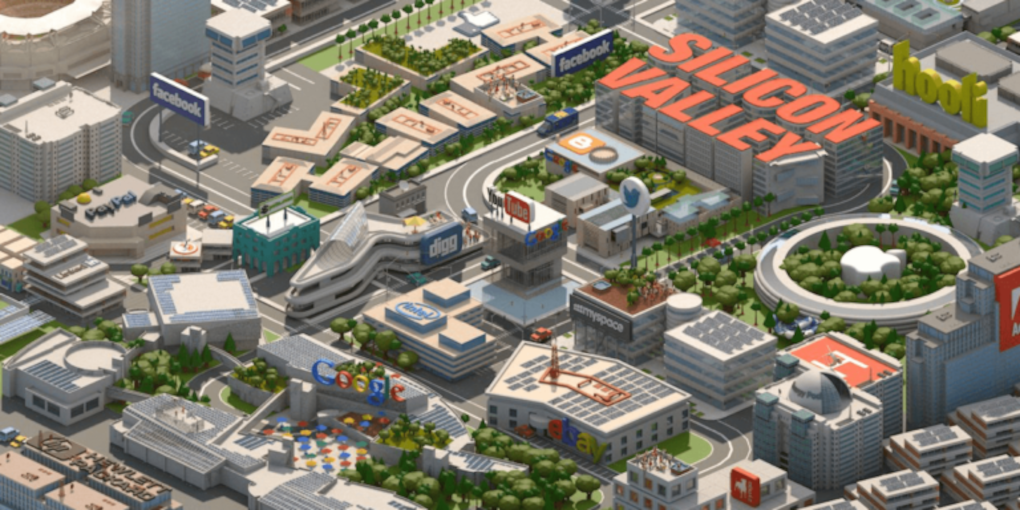
Upon arriving in Silicon Valley, I appeared fortunate compared to many students who came seeking education or individuals who had arrived even earlier to establish themselves. I had job stability and some savings. However, I was relatively older when I arrived, and economic pressures, career positioning, and future planning were all uncertainties. It was during this period of uncertainty that I became more proactive in accumulating knowledge for life and work, and cultivating my personal value. Ideally, such steps should have been planned during undergraduate or postgraduate studies, but for me, the uncertain environment pushed me to execute these actions efficiently.
As for how I obtained the transfer opportunity and whether there was competition, this question needs to be considered in the broader context. The United States is an immigrant country, and technical immigration is relatively direct and swift. Many international students stay in the United States through the H1B → EB2/EB3 path. Therefore, the door at the company level was always there;

Find me on Linkedin: @ICSteve
Related posts